Kipra Keyboard Build Guide
This guide will walk you through the process of building a kipra keybord.
Parts List
Caveat: parts availability changes quickly and vendor inventory tends to be come and go. Probably, you'll be able to get everything from 3 vendors, but some struggle may be involved.
- A pair of kipra v1 PCBs.
- I suggest PCBWay to fabricate boards for you
- The exact .zip file I uploaded to them is available in the focusaurus/kipra-keyboard github repo
- It's
kipra-v1.gerber.zipin the root of the repo
- a pair of RP2040 MCUs. I bought these on aliexpress - the 16M "color"
- these will come with pin headers
- 44 kailh choc switches
- I strongly endorse the new amazing Kailh Choc Ambient Nocturnal 20g linear silent switches from the fantastic lowprokb.ca store.
- lowprokb stocks most of the parts you need for this build
- 44 kailh choc hotswap sockets
- 44 keycaps of your choosing
- 44 diodes
- I suggest surface mount (SMD), but the board supports through-hole as well (in theory)
- a pair of TRRS connectors
- A TRRS cable. I suggest about 1 meter so it can run behind a laptop and 90-degree connectors make the most sense for that. If you know you want your cable to go straight across between the halves then a straight cable connector is fine.
Tools and Supplies
- soldering iron and solder
- small breadboard
- flush cutters
- masking tape and marker
- high quality precision tweezers
- safety gear if you are using leaded solder
- nitrile gloves
- fume extractor and/or respirator
- bins to hold tiny parts are very helpful
- excellent lighting and/or headlamp
- safety glasses
Study soldering technique and safety
If you are new to soldering, head over to youtube and watch some tutorials for technique and safety.
Flash the MCU ahead of time
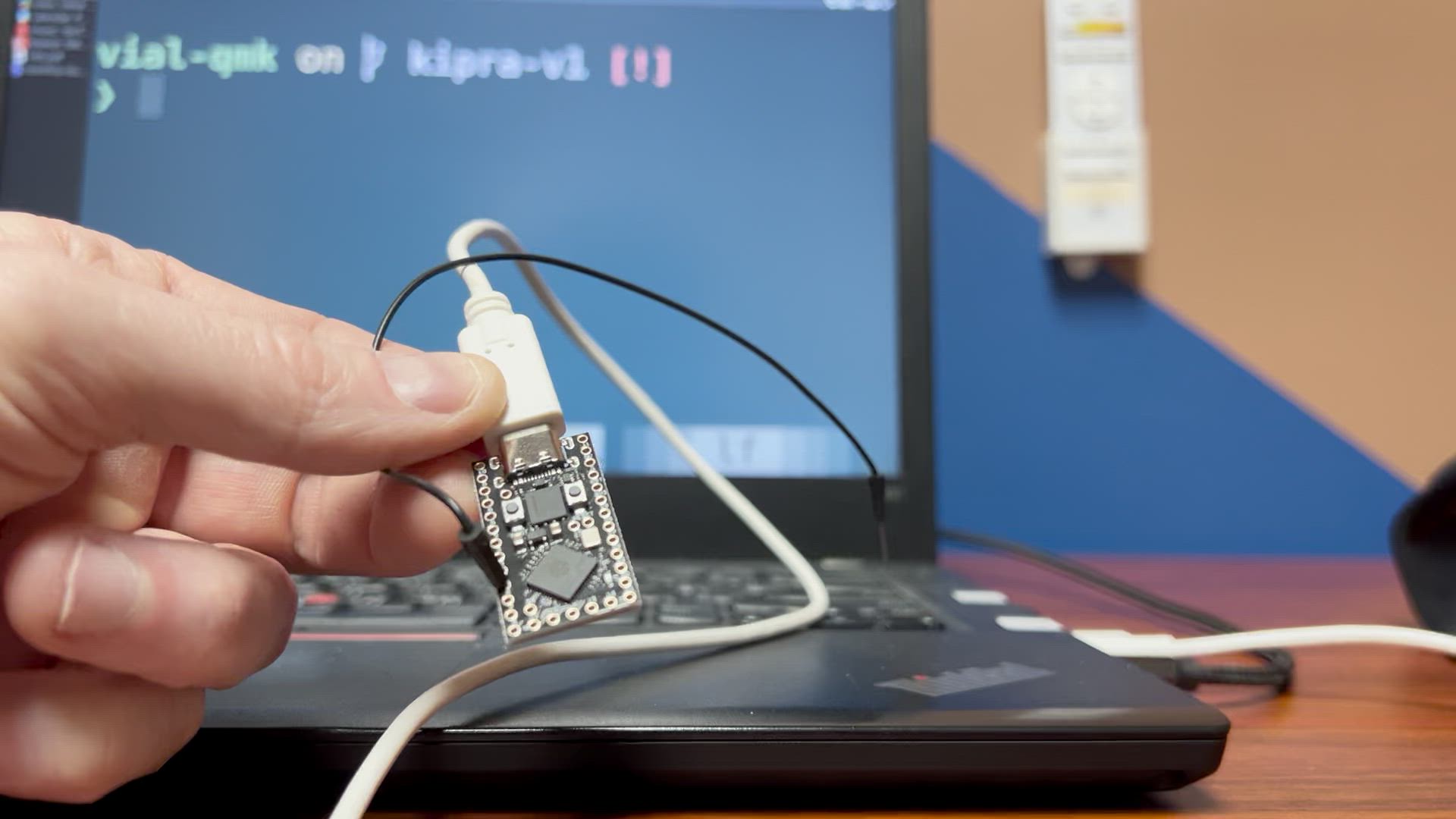
I suggest flashing the MCU as soon as you receive them. Better to get this sorted and out of the way so when you finish assembly, you get the satisfaction of having a working keyboard without any flashing frustrations spoiling the experience.
I have not yet published my QMK and Vial ports. If someone other than me ever actually builds one of these, hopefully I will have figured out how to do that either by merging the keeb into QMK and/or Vial or just adding them to the kipra repo on my github or something.
If you flash the bare MCU, you should be able to type letters by shorting through holes from the end of the left column to the end of the right column.
Build one half at a time
I recommend building only one half start to finish first unless you have a lot of experience building keyboard kits. This way you are more likely to make a mistake on only 1 PCB not both. Each half will work as a keyboard when connected to the computer via USB so you'll know everything is correct.
Steady hands
Pro tip: you might want to avoid caffeine on build day. My hands get shakier if I've had too much caffeine and these SMD diodes are tiny!
Label the PCBs halves and sides
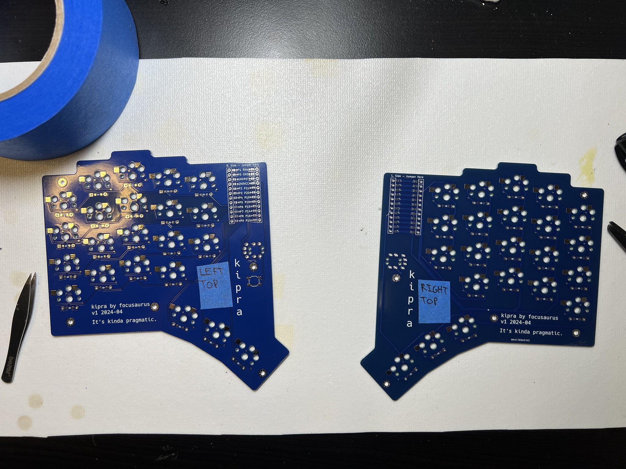
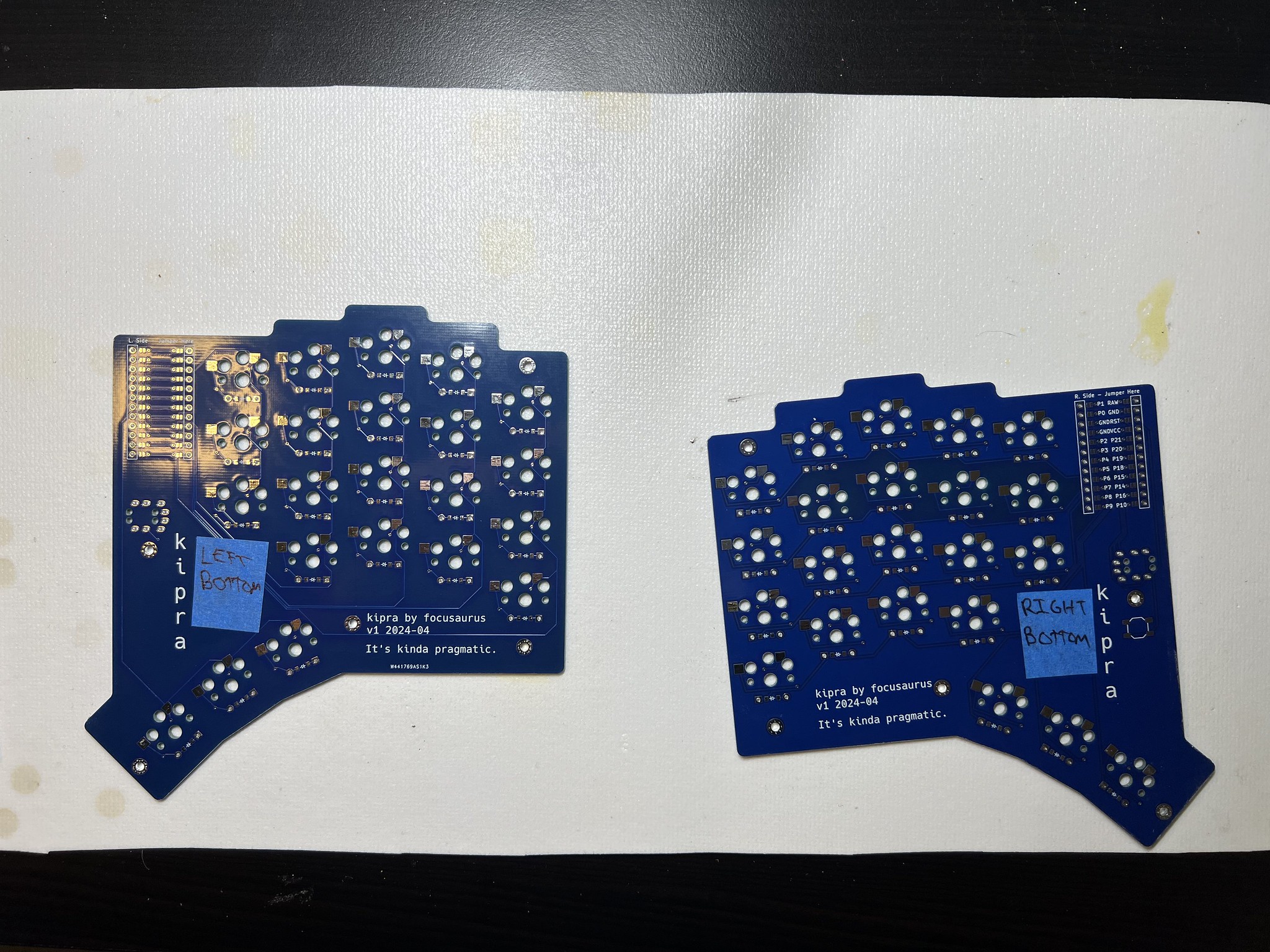
Take your PCBs, lay them out so you have a paired left and right, and put a piece of masking tape on them labeling all 4 sides: "left top", "left bottom", "right top", "right bottom". It's easy at the beginning of the build to lose track and solder something to the wrong side.
Solder the diodes
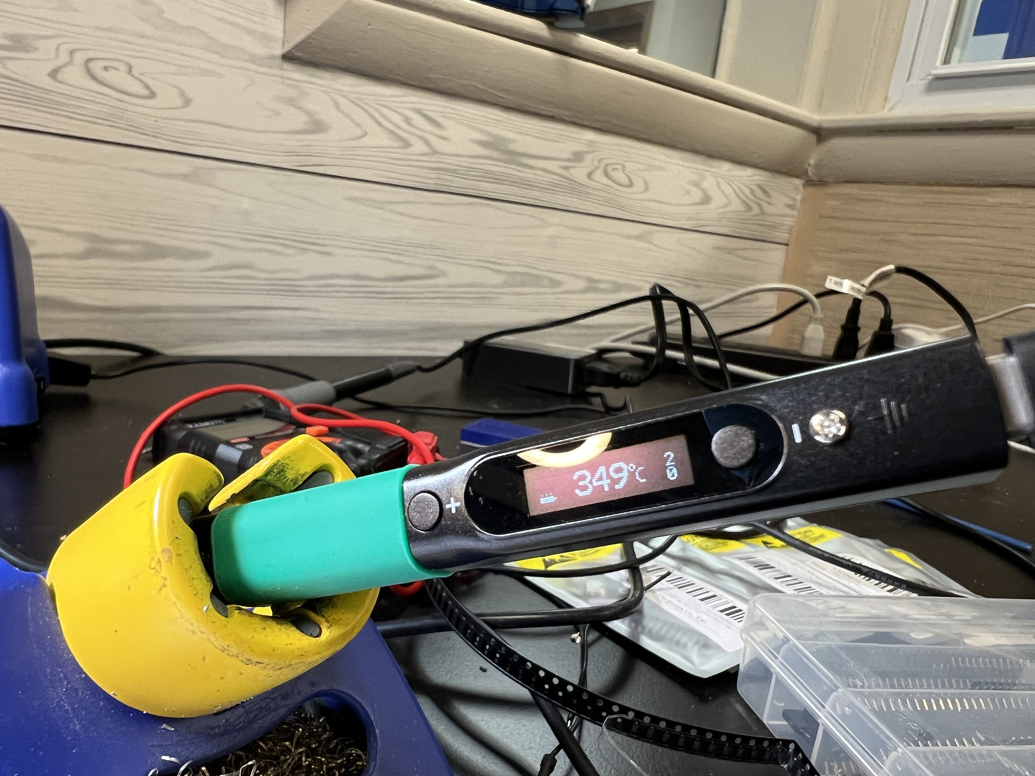
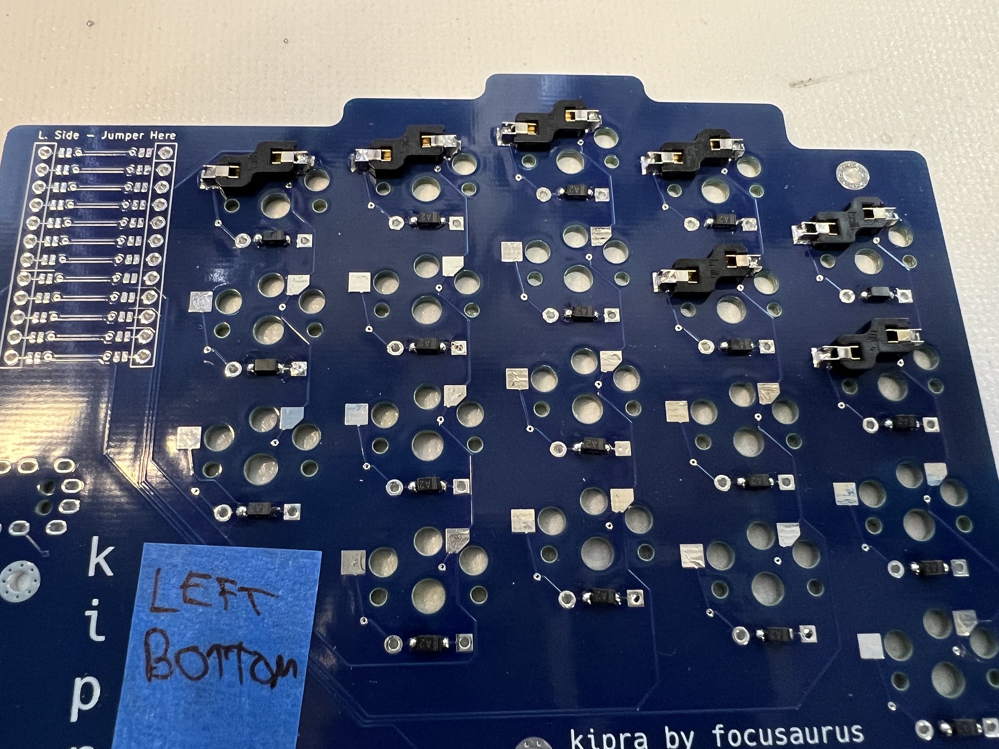
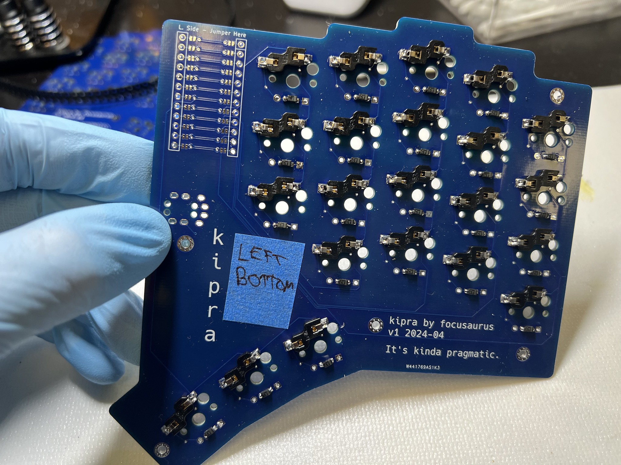
Set your iron to 350°C (or whatever works best with your solder, but as low as will work). The diodes go on the BOTTOM so make sure you are working on the bottom side. The stripe on the diode needs to align with the direction the arrow points on the PCB silkscreen. This is not symmetric so for the left half the text on the diode will be upside down, and on the right hand the text will be right side up.
For surface mount, heat one pad and put the tiniest amount of solder you can onto it. Then get the diode ready in tweezers butting up to that solder blob. Reheat it and slide the diode so the lead is in the solder and it's properly centered on the footprint. Hold it steady while you remove the iron. For the other lead, heat the pad & lead and solder them as normal.
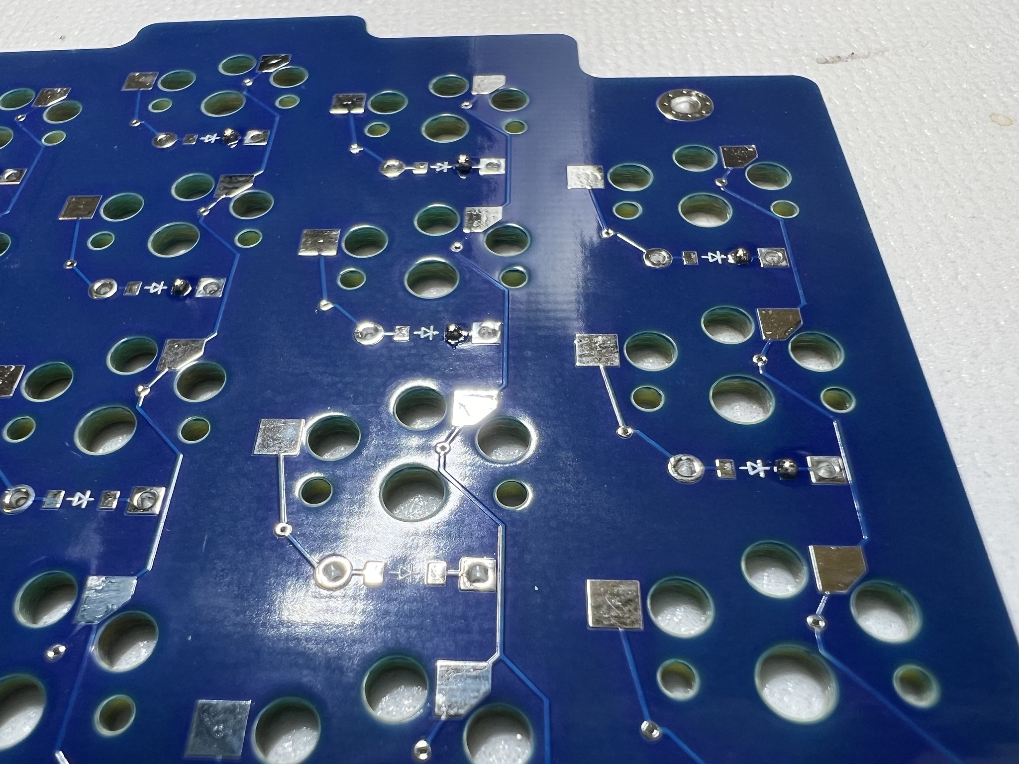
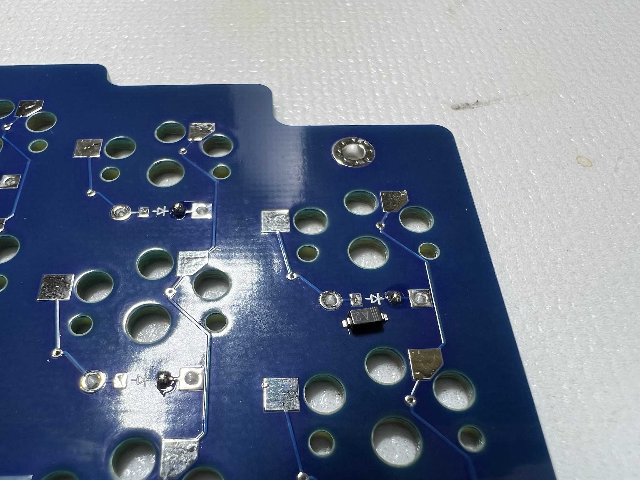
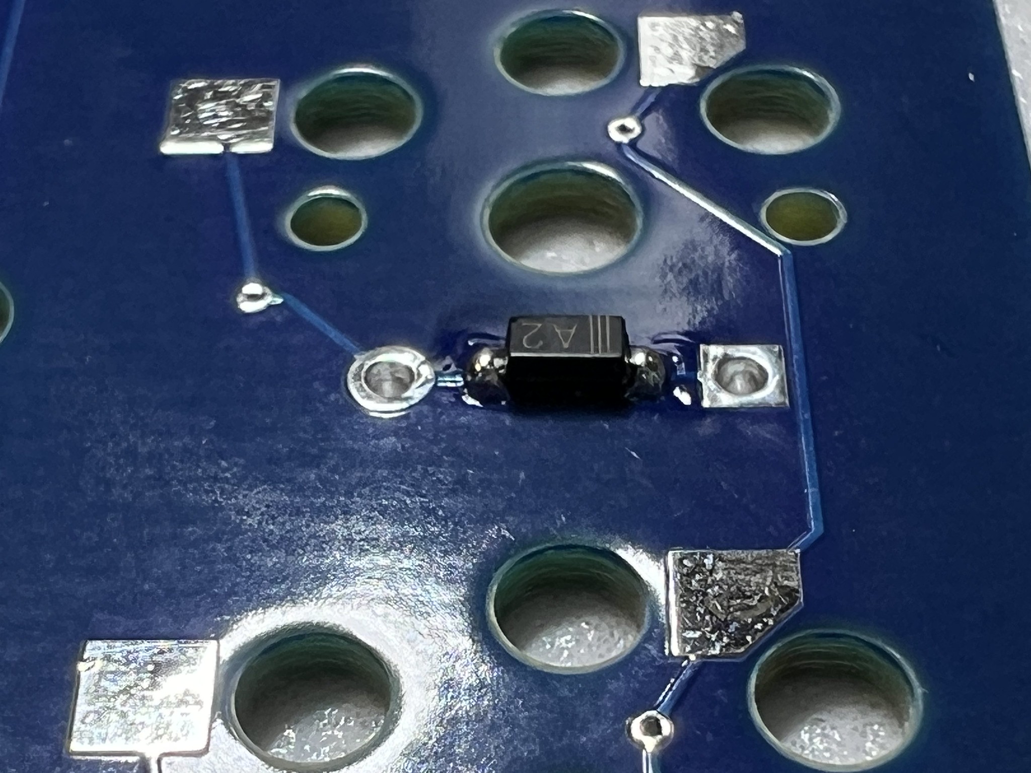
Continue for the rest of the diodes. After each row or column, do a scan to visually confirm they are all facing the same way.
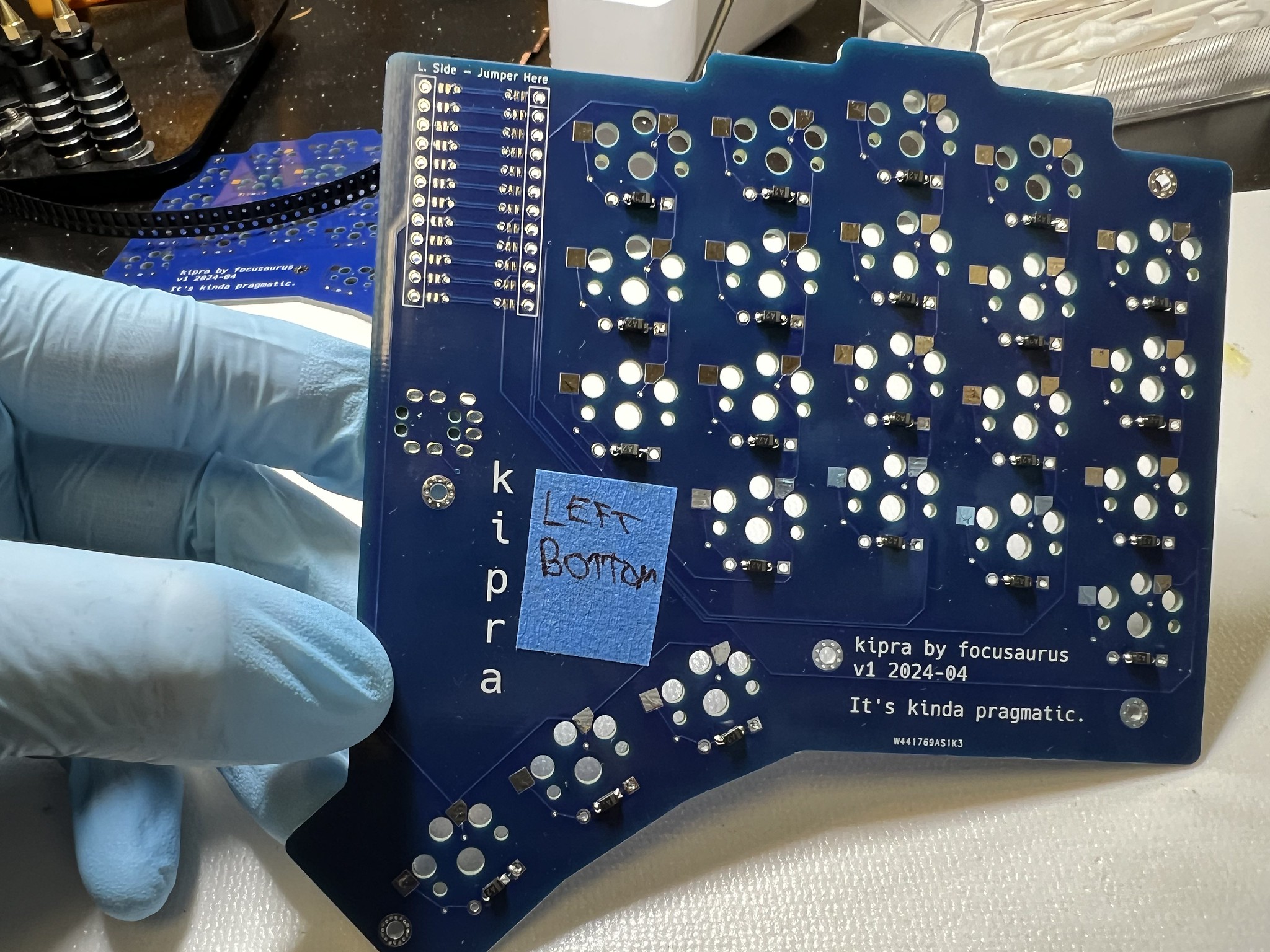
Solder the hotswap sockets
Still working on the bottom, install a hotswap socket. Heat one pad by shoving your iron into the metal bit of the hotswap socket and flood it with a decent amount of solder. Being careful not to burn yourself, use the tip of a finger to press the other side of the socket firmly down to be sure it's evenly seated before retracting the iron from the other side. Use tweezers or a pencil eraser or something if you are worried, but I was able to just use my finger and suitable amount of caution. Solder the other side and repeat for each key.
Solder the MCU jumper pads
Turn the PCB over so you are looking at the left top side. We are going to connect each pair of jumper pads within the MCU footprint. Heat both pads with your iron tip if possible and get a small dot of solder to cover both pads. Make sure when it cools there's enough solder so it doesn't shrink to 2 disconnected dots, but not a huge amount that might spill to a nearby pad or through hole. Note that the silkscreen instructions say "R. Side - Jumper Here" and this is the left side for us. This is OK. We want our MCU mounted face up so the buttons are accessible, but the footprint was designed primarily for folks who like to mount their MCU face down.
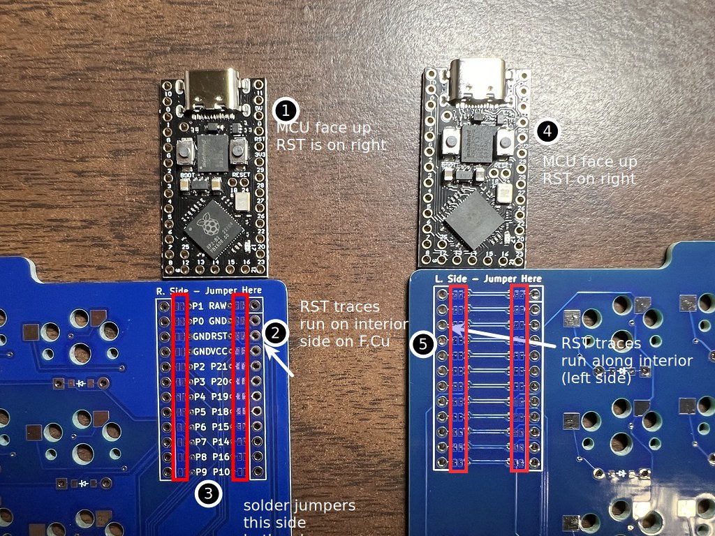

Continue until each pair of jumpers is connected.
Solder pin headers to the MCU
You can use socket headers if you like, but I'm not very concerned about moving my $4 MCU to another keyboard, so I just use normal pin headers. The MCU has 1 extra through hole compared to our PCB footprint, so you'll need to snip 1 pin header off the strip to have the right number.
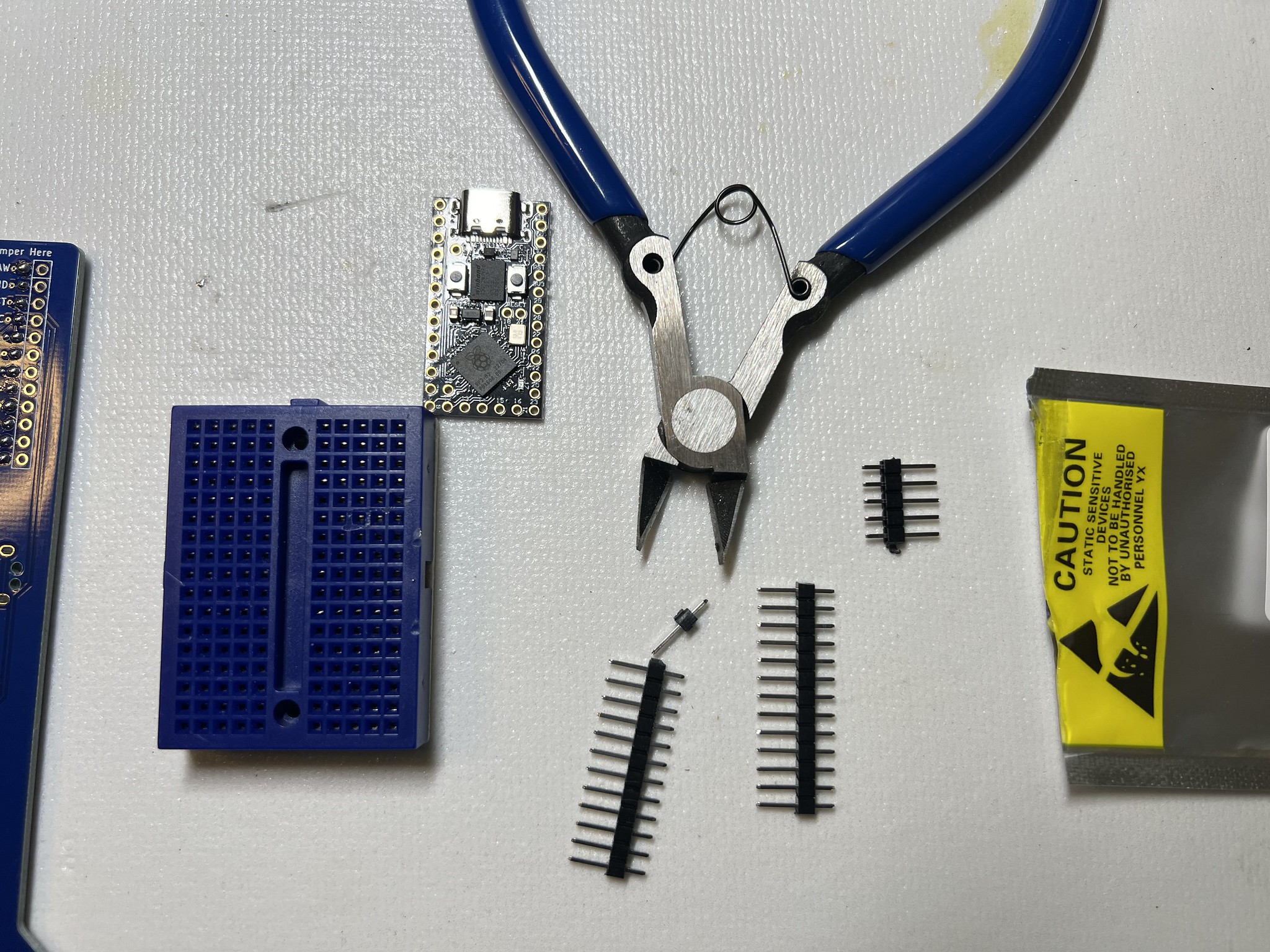
Set 2 columns of pin headers into a breadboard, longer section of the pin in the breadboard, shorter section sticking up in the air. Mount the MCU onto the pins with the empty pair of through holes closer to the USB connector. The through holes at the corners furthest from the USB connector should have pins in them. The MCU should be face up with the buttons visible.
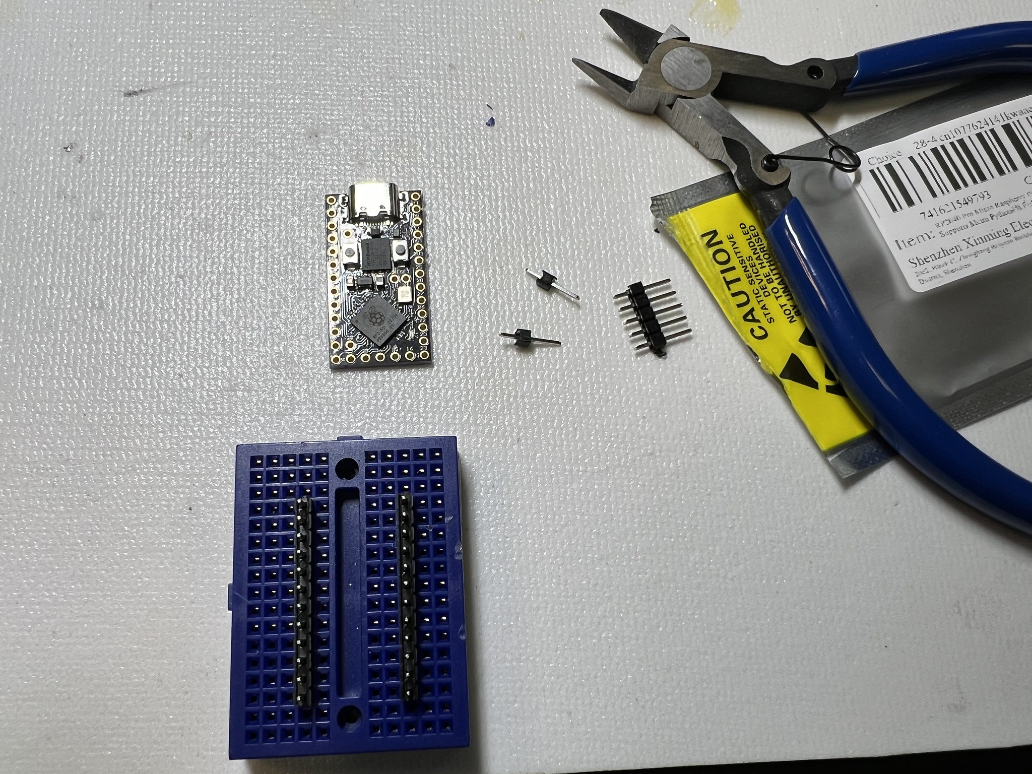

Solder the pin headers.
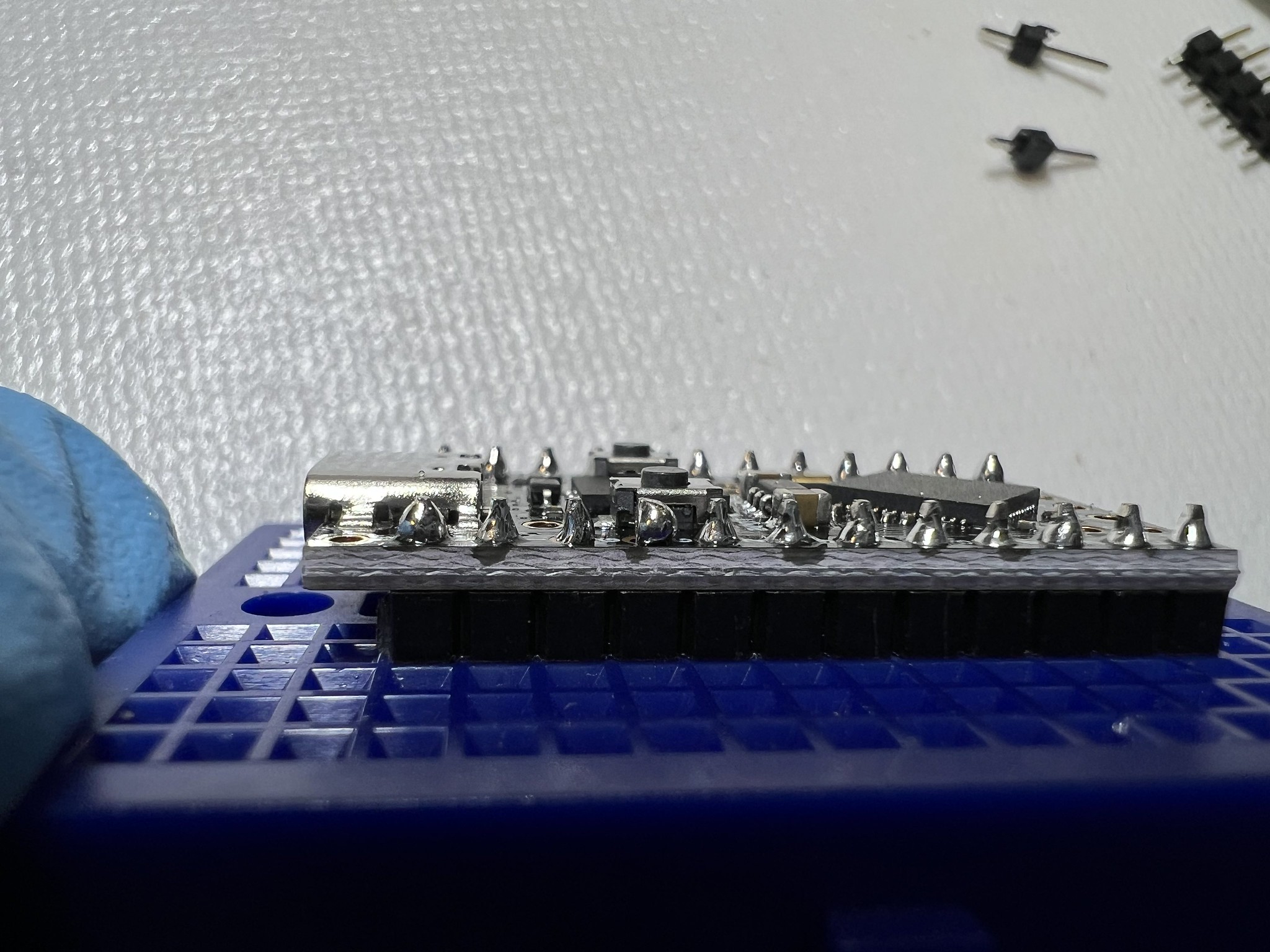
Solder the MCU to the PCB
Put the MCU into the PCB from the top then turn it upside down to solder from the bottom side.
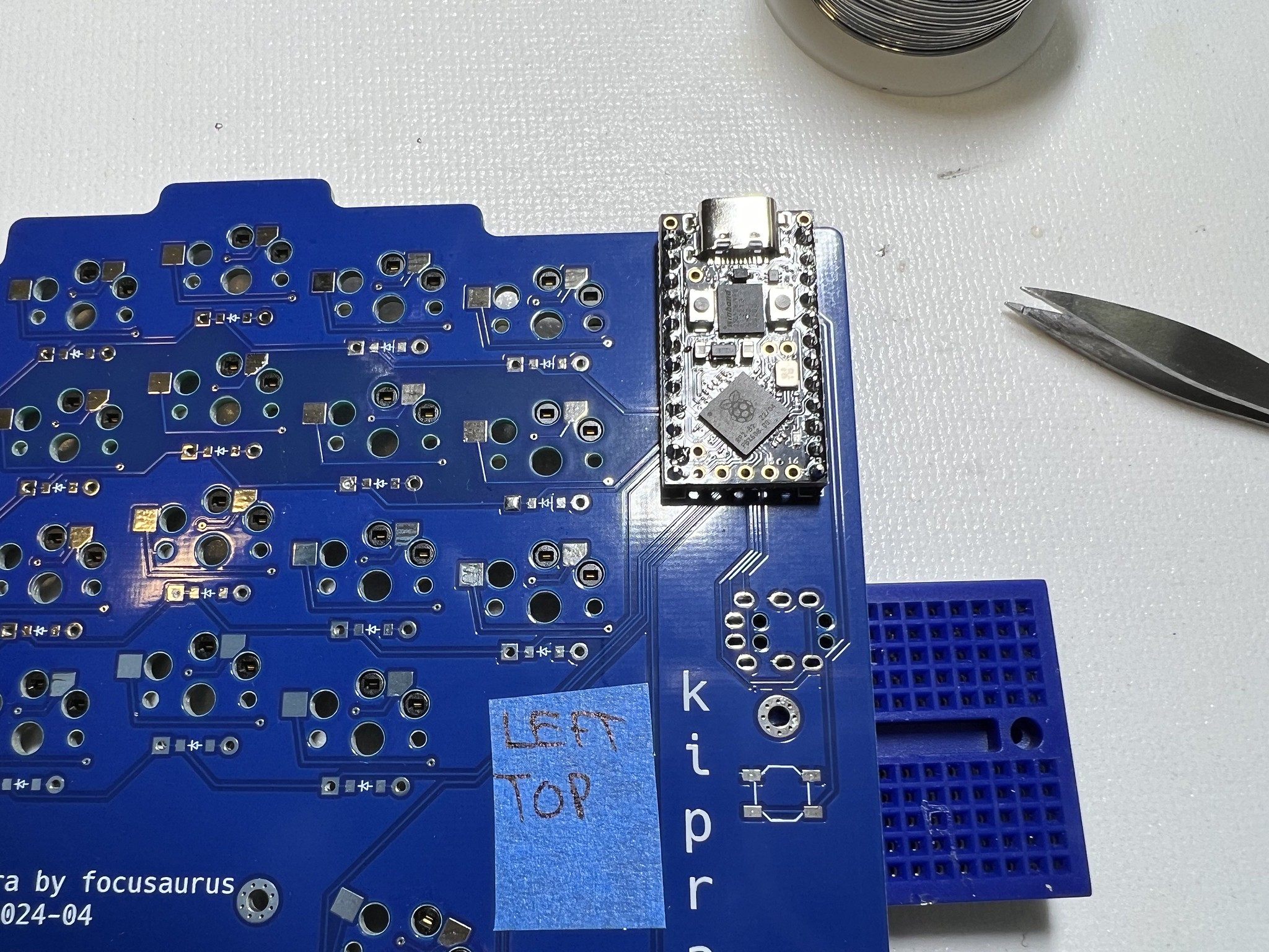
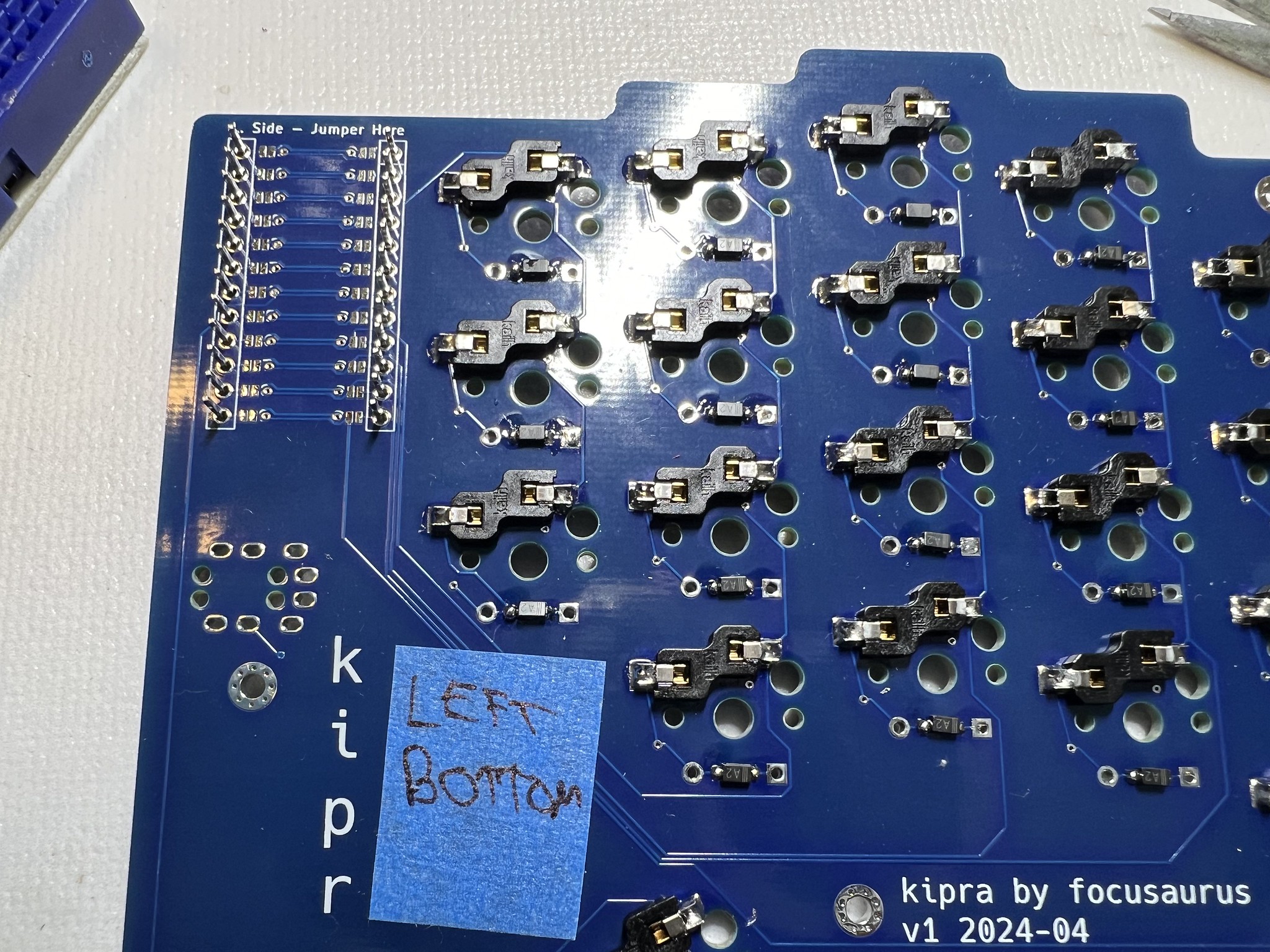
Solder the pin headers to the through holes.
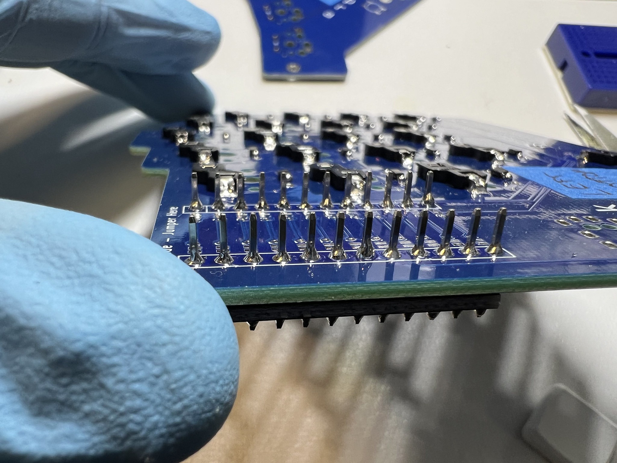
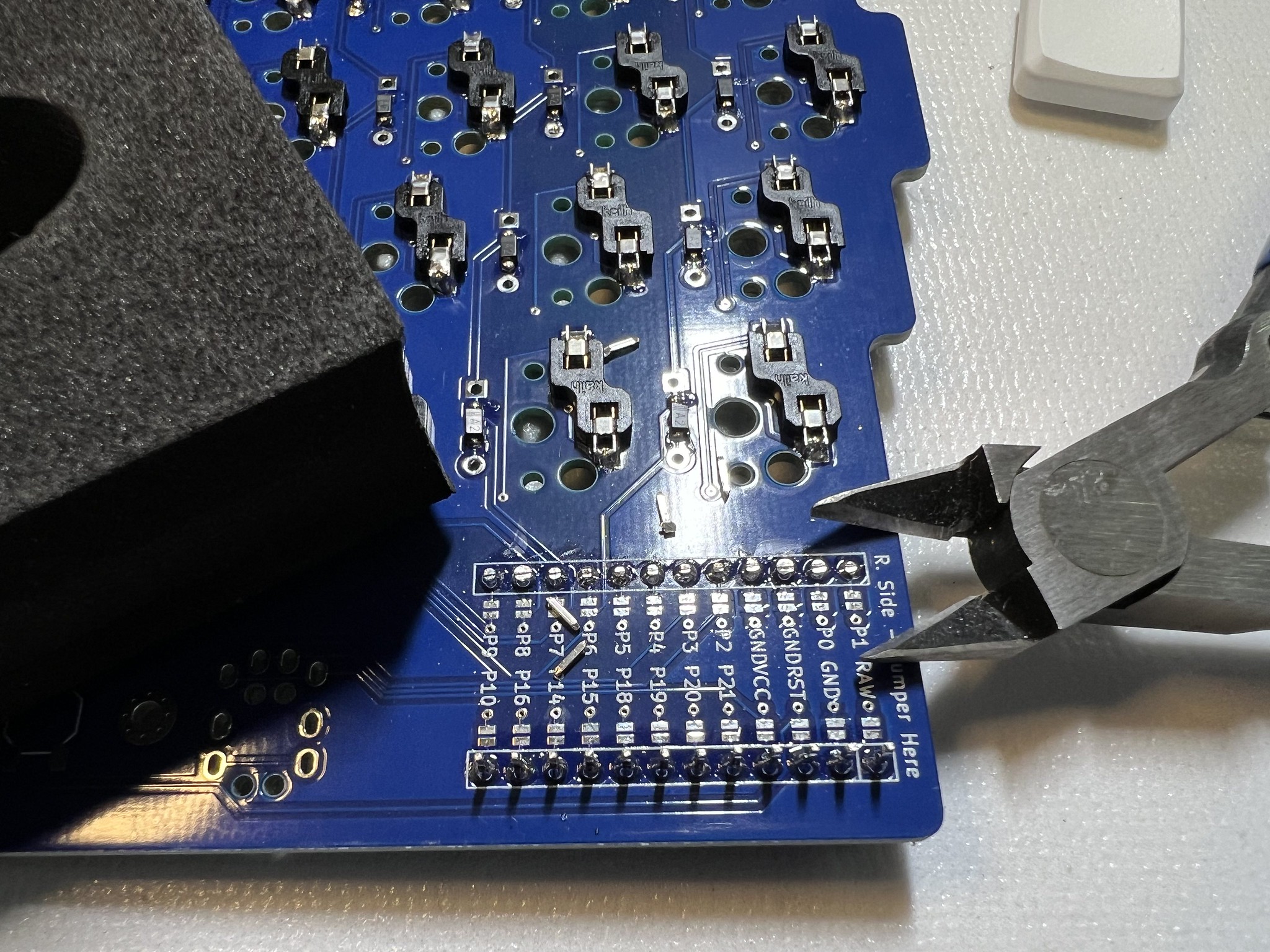
Next we'll trim these flush BUT these tend to fly off and really want to poke into your eyeball. Wear safety glasses and/or put something on top of the header to hold it in place while you trim it so it doesn't fly off. I used a little piece of dense packing foam that was lying around.
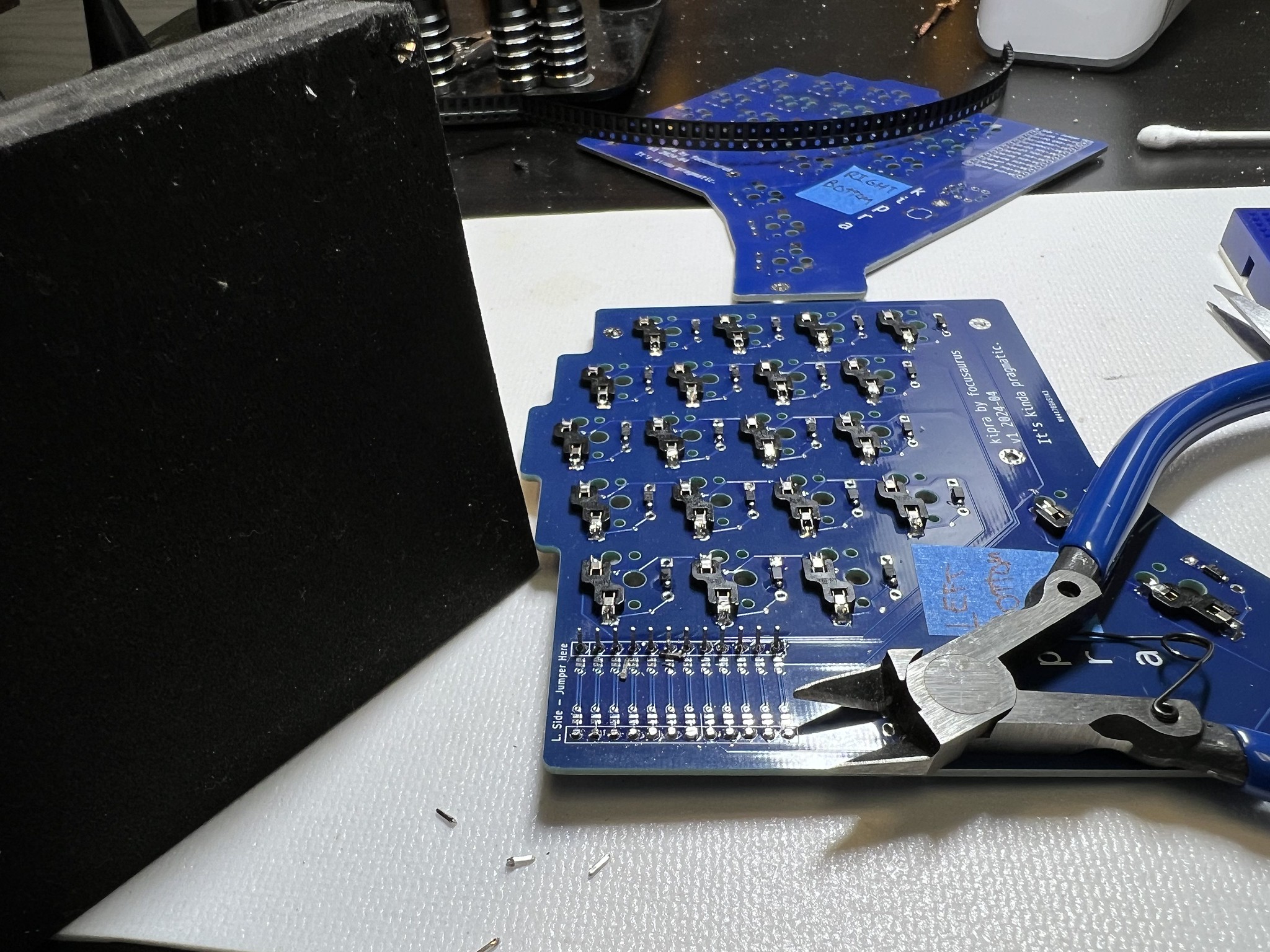
Solder the TRRS connector
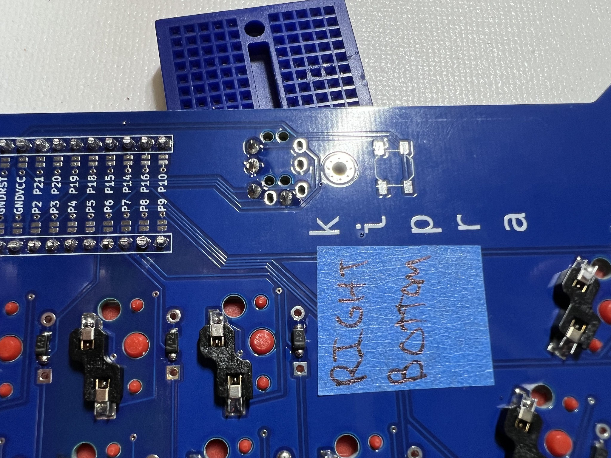
This mounts to the top side of the PCB and solders on the bottom. I rested the top of the TRRS connector on my breadboard to hold the connector flush against the PCB while soldering.
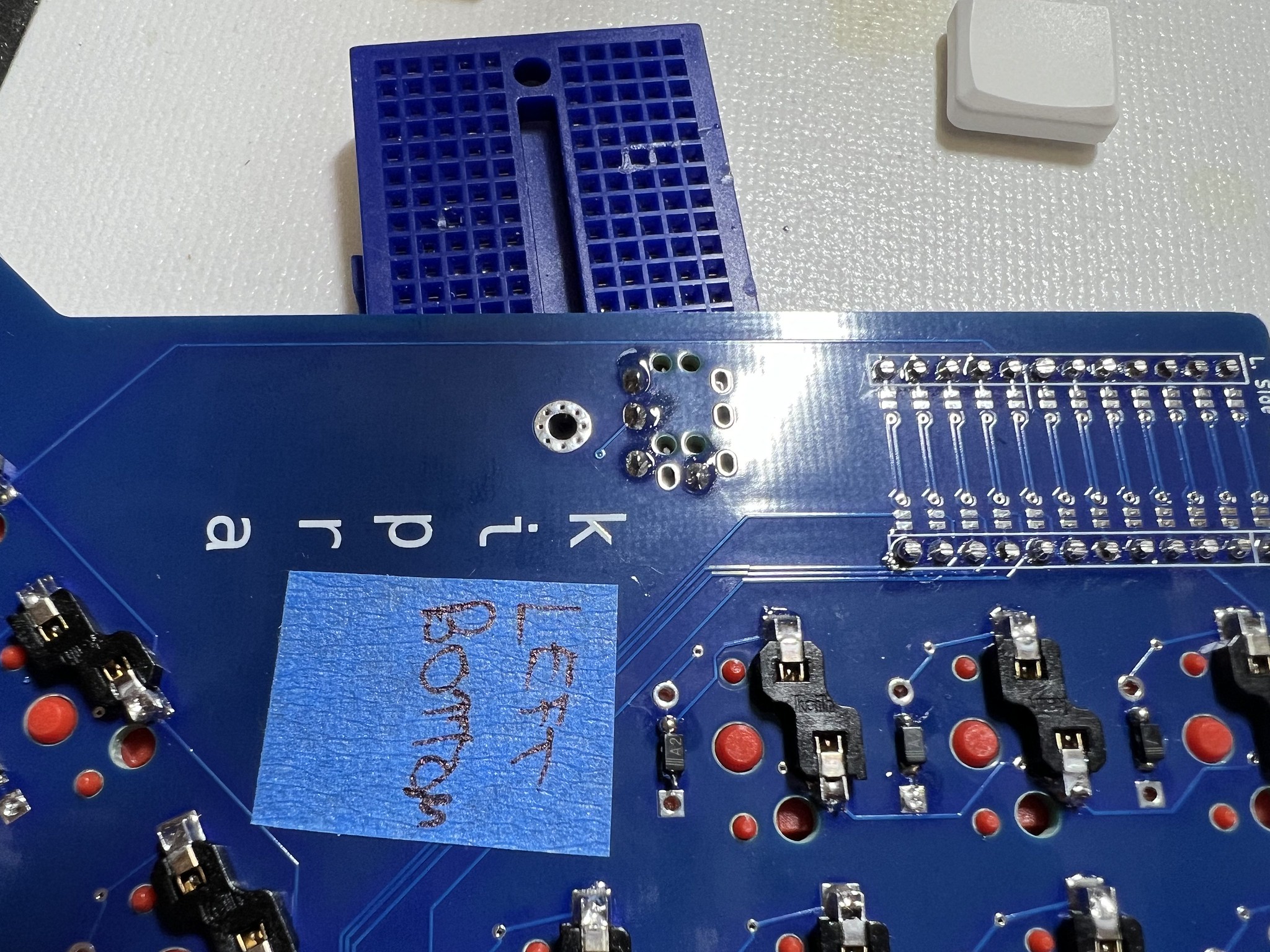
Install some switches
You can now install switches into the hotswap sockets. Make sure both switch pins are not bent and aligned properly to seat into the socket. I like to support the underside of the socket with my finger and press firmly to get each switch fully seated and flush but not put too much force on the solder joint for the hotswap socket.
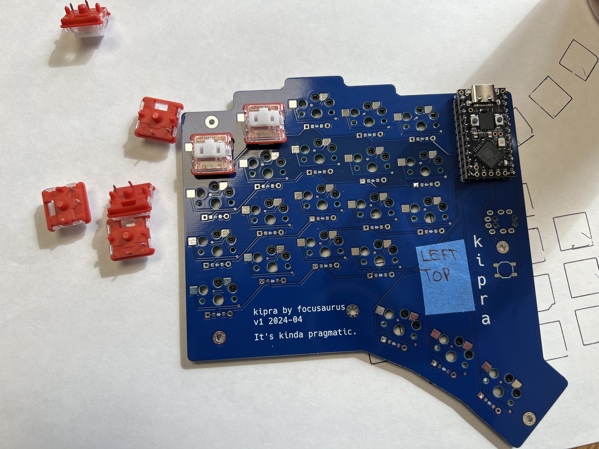
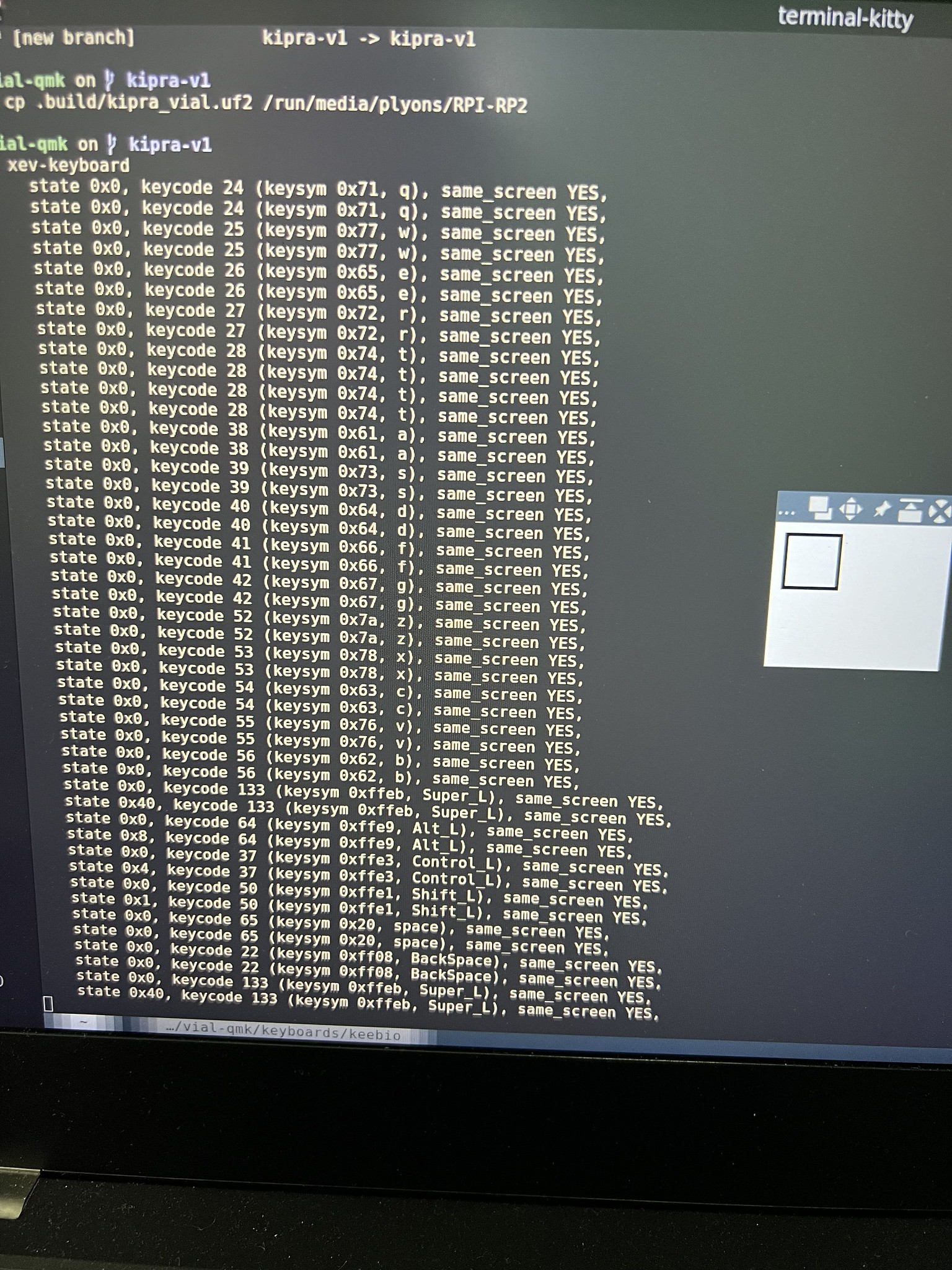
Plug it in and see if it types
You can now connect USB (assuming your MCU is already flashed with firmware) and it should type letters. If something doesn't work, check diode orientation. You may need to reflow some solder joints if anything is not working. Note the USB connector on this MCU is not mechanically very strong, so be gentle when plugging and unplugging it and take care you are moving the plug straight and level.
Take break
Rest your mind a bit if you intend to do both halves the same day.
Proceed to the right half
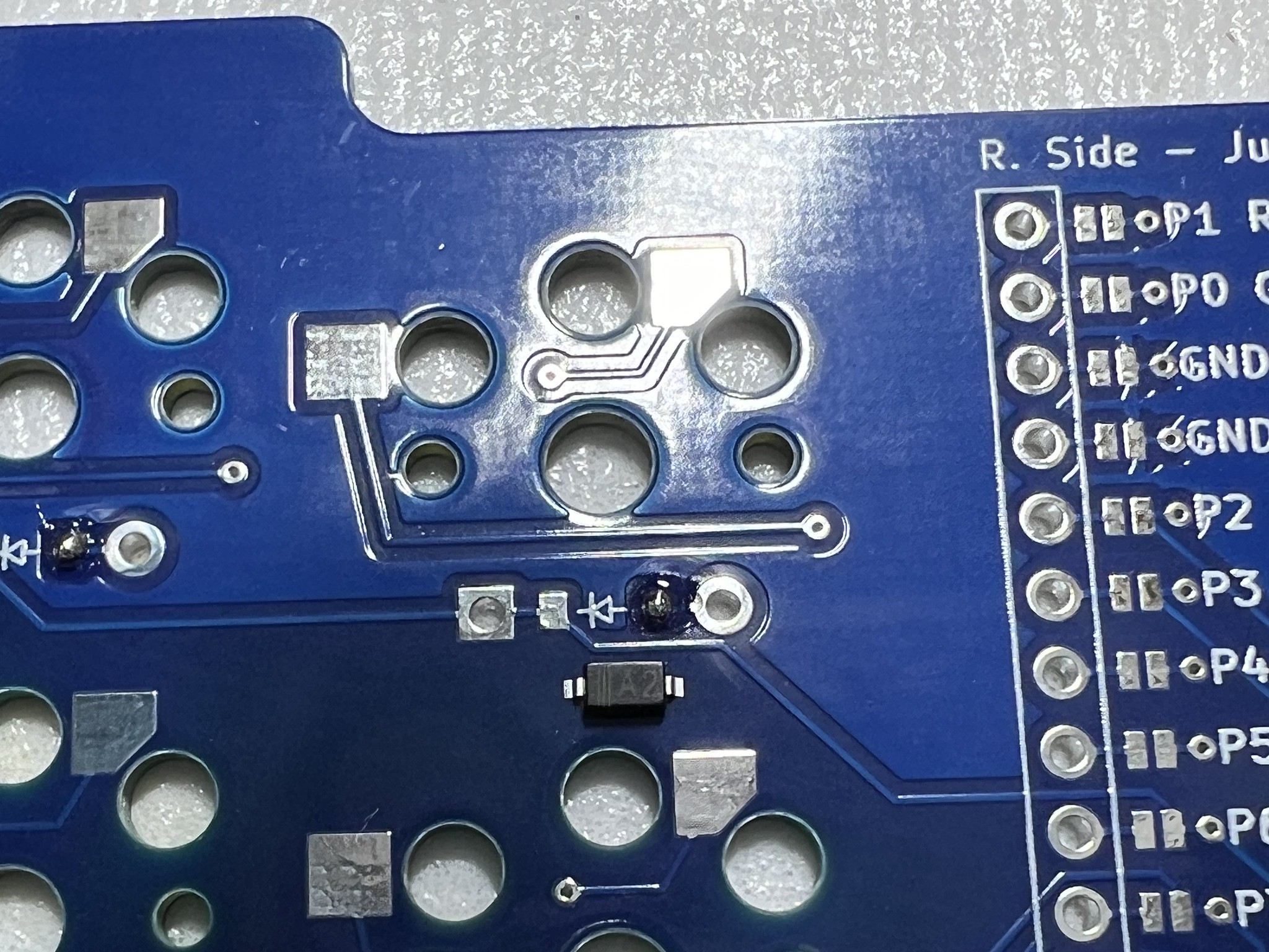
Right side diodes
NOTE the diode orientation will feel different on the right half. Make sure you are soldering them to the right half bottom side. The diode arrows will point left which means the diode label text will likely be right side up on this half of the keyboard.
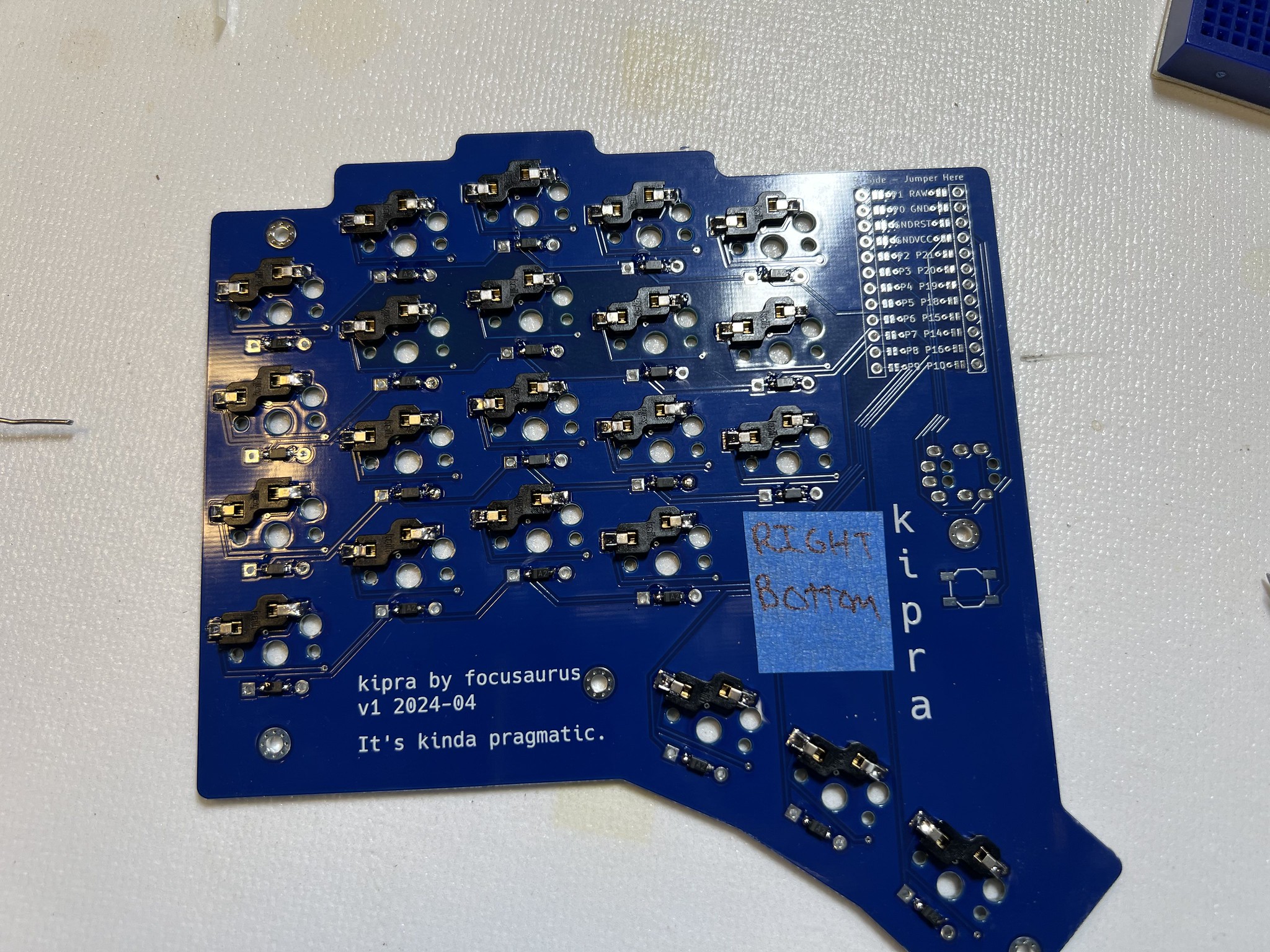
Right side hotwsap sockets
No surprises here.
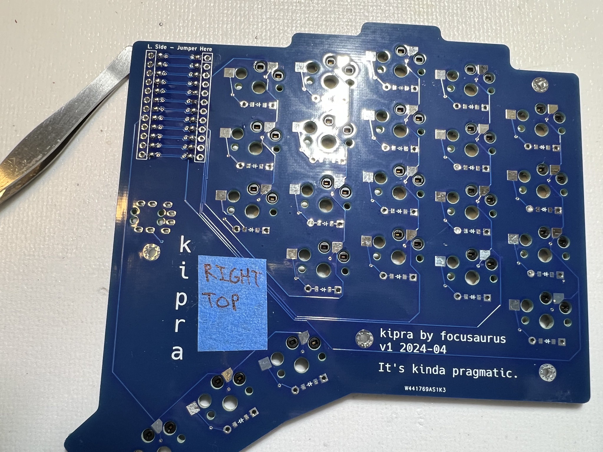
Right side MCU jumper pads
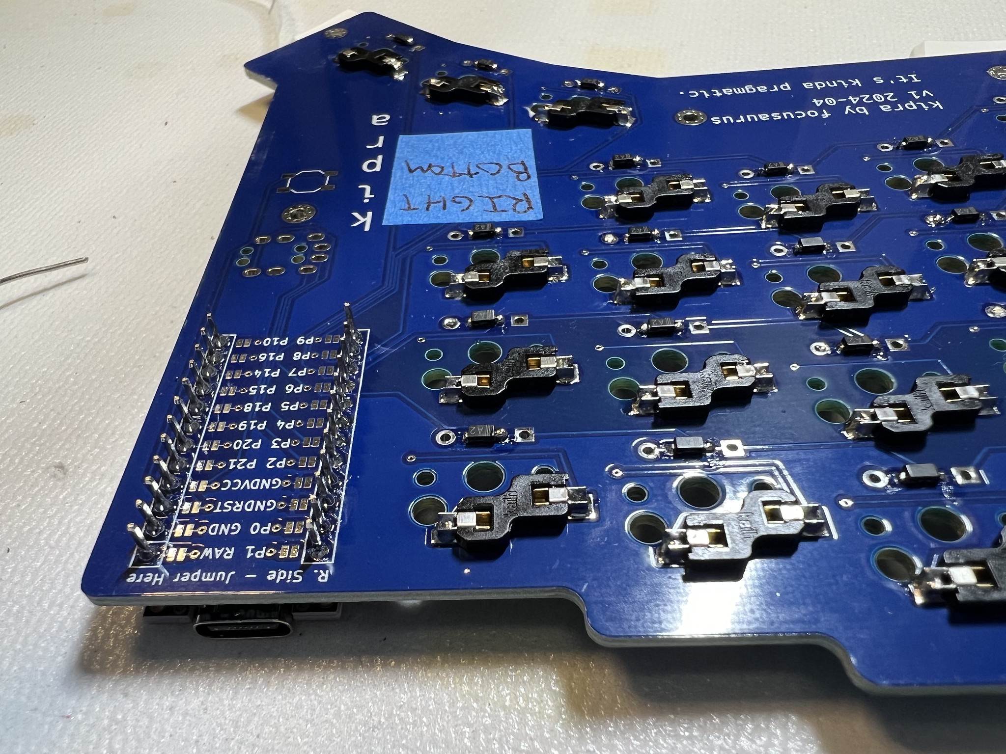
You will solder the MCU footprint jumper pads on the TOP RIGHT side. This is essentially "the same" as the left side, but it's tricky so I want to be clear about this.
Right side MCU to PCB
No surprises here. Buttons face up.
Flush cut the pin headers
No surprises here.
Right side TRRS connector
No surprises here.
Test the full keyboard
TRRS has an annoyance that the connector shape slides across a short circuit as you put the jack into the plug, so it's best to only connect/disconnect TRRS when USB is already disconnected. I've never seen this actually cause problems even after doing this wrong all the time on my ergodox for years, but I think it's a real thing that could damage your keyboard.
So connect the halves with TRRS, then connect the left half to USB. Both halves should work properly.

Add bottom liners
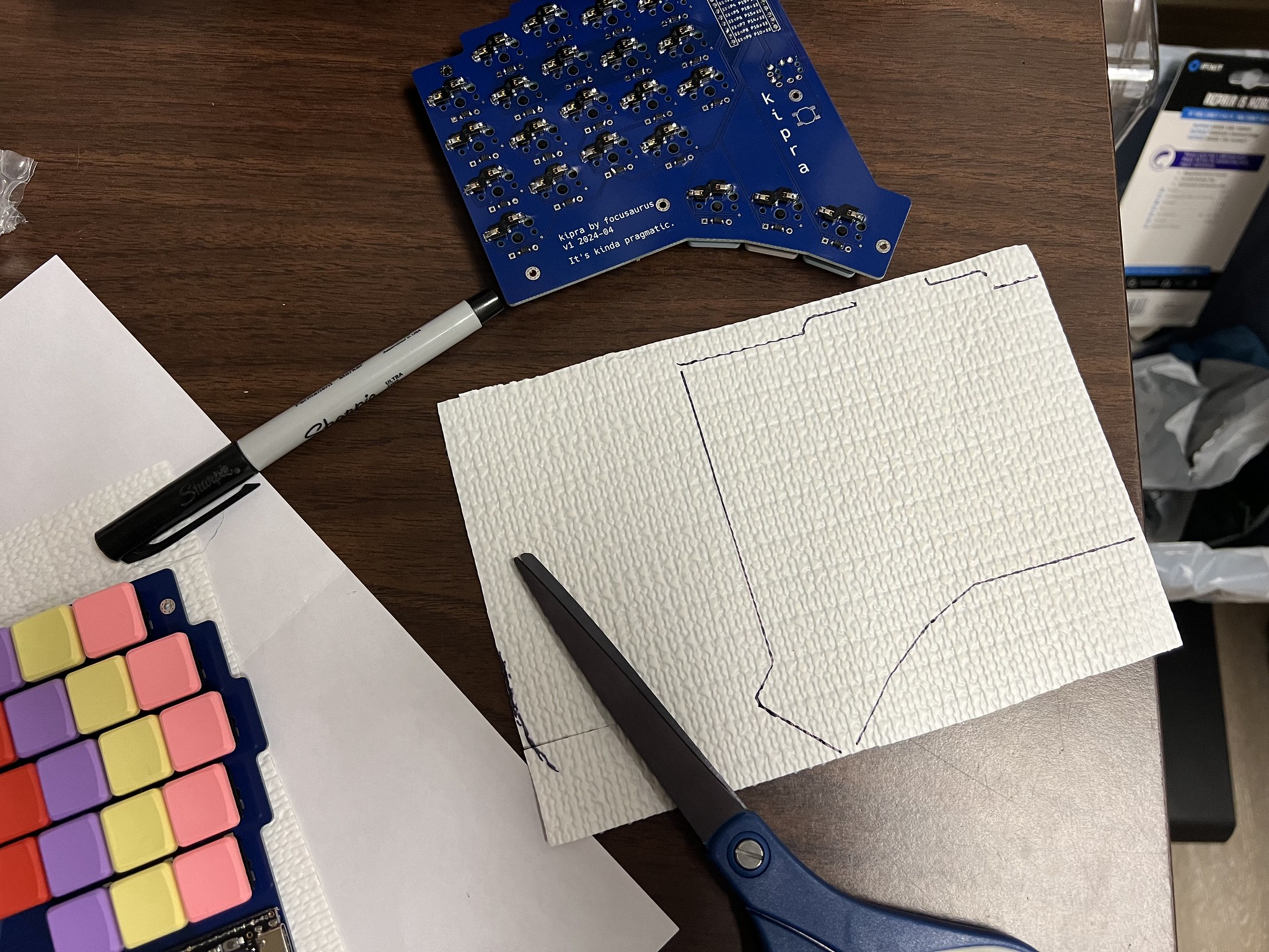
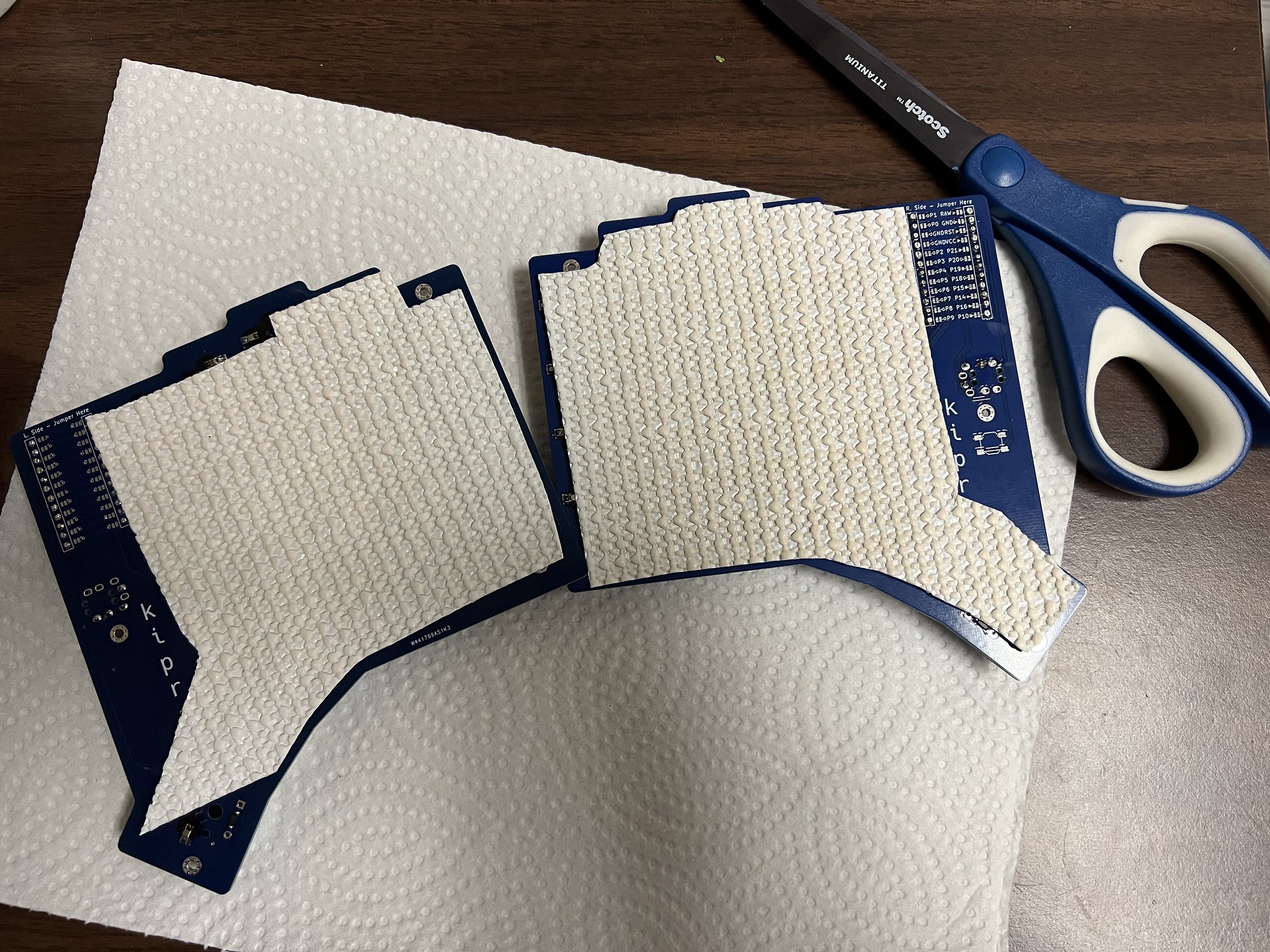
Perhaps the lowest-profile option for a case is no case. You may want to glue shelf liners to the bottom side for a little electrical shielding and a non-stick, non-scratch material for the desktop.
I cut my liners just a few mm smaller than the PCB shape and used some gorilla glue. I put the tiniest drop I could manage into the center of each hotswap socket, taking care not to get any glue into the actual socket. I spritzed the shelf liner with water which is how this glue says to do it. I left it with a little weight pressing it overnight to cure.
Done!
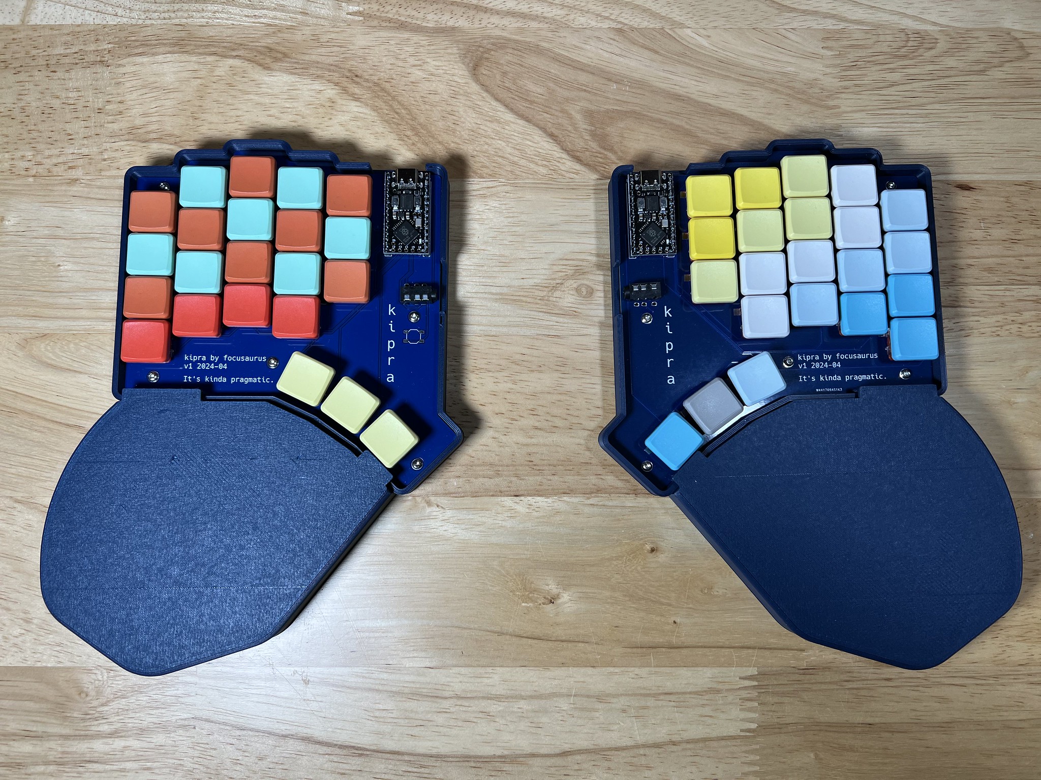
May your thumbs forever be untucked and your switches be silent!